
Product
Tel:0756-6180852
Sales Hotline:13798987404
Email:yuanyu_wei@test-way.com
Address:珠海市香洲区福田路10号博杰园区1栋

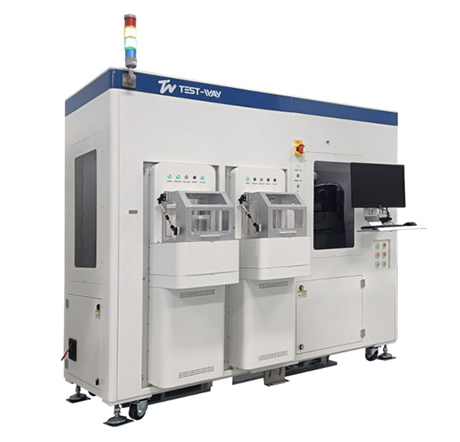
| Wafer Topography Inspection Equipment (Full-flat support) | WIS100 |
| Product Description | This non-contact optical wafer topography metrology system targets the grinding and polishing processes of compound semiconductor wafers. It accurately measures geometric parameters including wafer thickness, bow, global and local flatness. |
| Applications | 1.Substrate manufacturing processes: Monitor TTV、BOW, WARP and LTV after dicing, grinding and polishing of SiC, GaAs, InP and other substrates to ensure wafer uniformity 2.Pre-epitaxy quality inspection: Poor flatness leads to uneven epitaxial layer thickness. The system screens out defective wafers in advance 3.The equipment supports process monitoring and outgoing inspection for the above workflows |
| Inspection Method | Non-contact optical sensor |
| Applicable Materials | Compound semiconductor wafers (SiC, InP, GaAs, GaSb, etc.) |
| Holding Method | Flat support with vacuum chucking |
| Wafer Size | 2~8 inch, expandable to 12 inch (12-inch version requires custom development) |
Repeatability | 0.1μm 3sigma (TTV、LTV) |
| Measurement Precision | 0.1μm |
| Output Format | Intuitive data display with 2D or 3D mapping |




 Wechat